- Table of Contents
- 1. Introduction
- 2. Basic architecture
- 3. Physical Construction
- 4. Programming
- 5. Sample programs
- List of Tables
- 1-1. Specifications
- 2-1. Memory Reference Instructions
- 2-2. OPR Instructions
- 2-3. IOT Instructions
- List of Figures
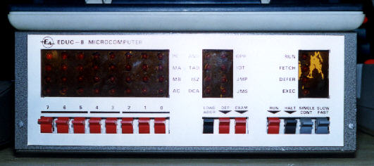
- 1-1. The EDUC-8
Chapter 1. Introduction
Note: Image from ACMS
The EDUC-8 is a TTL-based 8-bit microcomputer. It was designed by Jim Rowe and construction details were published in Electronics Australia magazine between August 1974 and January 1975. Additional peripherals were described in further articles up to August 1975.
The internal implementation is bit-serial which gives good economy of components as most data paths are only 1 bit wide. It does mean that processing is rather slow, as 24 clock cycles are required to perform one major cycle, and 2 or 3 major cycles are required per instruction.
Technically it might not be a microcomputer as it is not based on a microprocessor, but it seems to be stretching things a bit to call it a minicomputer and in any event the original articles referred to it as a 'micro-computer'.
My page for the EDUC-8 is at http://www.ljw.me.uk/educ8
Chapter 2. Basic architecture
The EDUC-8 is based on the DEC PDP-8 (which was a 12-bit machine). It has a similar instruction set and op-code layout, but because of the shorter instruction words there are fewer instruction variants and more limited addressing. In particular there is no link/carry flag.
Registers
Accumulator (AC)
The AC register is used to hold values for computation, loading and storing. It is the only register which the programmer can explicitly control.
Memory Buffer (MB)
The MB register is used to hold values which are being stored into memory, or have just been read from memory, including instructions.
Memory Address (MA)
The MA register is used to hold the memory address which is being used to reference memory, including instruction addresses.
Instruction Execution
A standard instruction requires two cycles to execute.
Fetch, during which the instruction is fetched and decoded
Execute, during which the instruction is processed
There is an addition cycle type, Defer, which appears between Fetch and Execute if indirect addressing is used.
Memory Addressing
Direct Addressing
Most instructions have a 4-bit address specifier. This can be used to refer to a memory address in the same 16-byte memory page as the instruction:
Addr = PC[7:4] + Instruction[3:0]
Indirect Addressing
To provide more flexible addressing and the possibility of indexing, instructions can optionally specify indirect addressing. In this case the final memory address is obtained by reading the location specified by the 4-bit address:
When an instruction uses indirect addressing, an extra DEFER cycle is required for the additional memory access.
Addr = Mem( PC[7:4] + Instruction[3:0] )
Front Panel
The front panel contains LEDs to display register contents, instruction type and run status. It also has switches to set register and memory contents, and to start and stop program execution.
Instruction LEDs
8 LEDs indicate the current instruction as AND, TAD, ISZ, DCA, JMS, JMP, IOT or OPR.
Entry switches
8 switches can be used to set the value of the PC register (using the LOAD ADDR switch) or the memory at the address specified by the PC register (using the DEP switch).
The switches are divided into groups of 3,2,3, which match the instruction layout with the top 3 bits being the opcode. This leads to program listings being represented in a 3,2,3 octal format, rather than the more conventionsl 2,3,3 format for an 8-bit number.
Control Switches
LOAD ADDRess sets the PC register to the switch settings.
DEPosit stores the switch settings in the memory location specified by the PC register, and increments the PC register. The MA register contains the address which has just been written.
EXAMine reads the memory location specified by the PC register into the MB register, and increments the PC register. The MA register contains the address which has just been read.
RUN starts program execution at the address specified by the PC register.
HALT stops program execution at the end of the current instruction, leaving the PC register pointing at the next instruction ready for re-starting with the RUN switch.
SINGLE/CONTinuous selects whether the program should run continuously when RUN is pressed, or only execute one instruction for debugging purposes.
SLOW/FAST selects the rate at which instructions are executed, with the slow setting reducing the clock rate from 500kHz to 2Hz.
Input/Output
The EDUC-8 has 4 serial I/O links, 2 input and 2 output. Devices designed along with the computer are:
Input
Paper-tape reader
Octal Keypad
Keyboard
Output
Paper-tape punch
Printer
Octal display
Music player
Burroughs self-scan display panel
Bidirectional
Asynchronous Current-Loop interface
FSK tape interface
Instruction format
Each instruction is one byte. The top 3 bits of an instruction are always the opcode. There are three types of instruction layout for the remaining 5 bits.
Full instruction details are given in Chapter 4.
The opcode can be from 000 to 101 (binary). The Ind flag is set to specify indirect addressing.
Bit 4 specifies which group of functions can be selected. Bits 3 through 0 specify a combination of the 4 different functions, though not all are meaningful.
Bit 4 specifies whether the Input (0) or Output (1) devices are used. Bit 3 specifies which of the two devices (2 input, 2 output) should be used.
Chapter 3. Physical Construction
The EDUC-8 is constructed of 8 circuit boards:
Front panel
11 ICs, 44 LEDs and 15 switches
Mother board
A passive board with connectors for the following 6 boards
Timing
21 ICs to generate timing and synchronisation signals for instruction execution
Instruction Decoder
14 ICs to generates control signals for the following boards depending on the current instruction and timing
Memory
256 bytes of volatile memory in two 256x4 devices, with another 16 ICs
Program Counter and Adder
14 ICs hold the PC register and provide a 1-bit serial adder used to increment the PC and AC as required
Accumulator
10 ICs mean this is the simplest of the boards
Input/Output
11 ICs to provide the four I/O channels
Chapter 4. Programming
Instruction Set
For memory reference instructions, the address is computed as:
Addr = (PC AND 11110000) OR (instruction AND 00001111)
and provision for indirect addressing:
If (instruction AND 00010000) > 0 Then Addr = Mem[Addr]
Note that the PC value used here is that of the instruction itself, the increment occurs afterward.
After each instruction fetch there is an implied:
PC = PC + 1
between fetching the instruction and executing it.
All addition is modulo 256.
JMS
Jump to Subroutine
The return address is stored in the target location, and execution commences from the next location.
To return, do a JMP I Entry
Re-entry is not possible unless you save the address somewhere else!
Mem[Addr] = PC
PC = Addr + 1
OPR Group
Operate
Instructions from the same group of 4 can be combined. Execution of functions takes place from Bit 3 to Bit 0.
IOT Group
I/O Transfer
There are 2 input devices and 2 output devices. The device number (0 or 1) is specified by bit 3 of the instruction.
When an I/O device is ready to transfer data, it sets a flag. This flag is checked by the SKF and SDF instructions, and reset by the RKF and RDF instructions.
Chapter 5. Sample programs
Counting program
This program increments AC 256 times, and after each increment loops 256 times to provide a delay.
START,  LA          / clears AC
INCR,   IAC         / increments AC
BACK,   NOP         / delay
        NOP         / delay
        ISZ INDX    / loop on INDX
        JMP BACK    / if INDX non-zero
        ISZ INDY    / loop on INDY
        JMP INCR    / if INDY non-zero
        HLT         / INDY is zero
INDX,   0           / Delay counter
INDY,   0           / Follows AC
Paper-tape punching program
This program accepts 3 digits from the numeric keypad (Input device 0) while displaying them on the 7-segment display (Output device 0), and if the LF key is then pressed the specified byte is punched onto paper tape (Output device 1). If a fourth digit key is pressed instead of LF, the display is cleared and no byte is punched.
READ,   0           / Read byte from keypad subroutine
TEST,   SKF
        JMP TEST    / Loop until byte ready
        KRB         / Read it
        JMP I READ  / Return
BUFF,   0
START,  RKF
        JMS READ    / Get first digit 'A'
        DCA BUFF    / Store it
        TAD BUFF    / Get it again
        LDB         / Display digit 'A'
        TAD BUFF    / Get digit yet again
        RAL
        RAL         / Multiply by 8
        DCA BUFF    / Save it
        JMS READ    / Get second digit 'B'
        TAD I BUFD  / Combine with first
        RAL
        RAL
        RAL         / Multiply by 8
        DCA I BUFD  / Save
        TAD I BUFD  / Reload
        LDB         / Display digits 'AB'
        JMS I REDD  / Get third digit 'C'
        TAD I BUFD  / Combine with first two
        DCA I BUFD  / Save
        TAD I BUFD  / Reload
        LDB         / Display digits 'ABC'
        JMP I CONT  / Jump to loc 040
CONT,   040         / Points to following instruction
REDD,   000         / Points to read-byte subroutine
BUFD,   005         / Points to BUFF
        JMS I REDB  / Get command digit (this is loc 040)
        SMA         / Punch?
        JMP SCRB    / No, Scrub
        CLA
        TAD I BUFB  / Get the byte
        LPB         / Punch it, LPB = LDB for second device
CHEK,   SPF         / SPF = SDF for second device
        JMP CHEK    / Wait for it to be punched
SCRB,   CLA
        LDB         / Clear display
        JMP I STAD
REDB,   000         / Read-byte subroutine
BUFB,   005         / BUFF
STAD,   007         / START